
To fabricate a prototype of a IC chip is very expensive and it needs from several months up to 1 year to be finished. WHY???
Let’s explore all the designing steps that a CHIP requires…

The fabrication of a prototype IC chip is a highly costly and time-consuming process, requiring significant financial investment and an extended timeline ranging, at least, from several months to even a year for completion.
Imagine, it is like pressing the printing button once the chip is fully designed on the computer
The tape-out of a chip prototype is a very costly and long process. Consequently, it becomes crucial for designers to strive for a successful tape-out without the need for re-design iterations, whenever possible.
In today’s highly competitive market, companies are continuously seeking ways to minimize their time-to-market and launch new products while also reducing costs. On the other hand, research institutes and universities often operate under budget constraints, limiting their ability to engage in multiple tape-outs throughout the year, typically being limited to 1 to 3 tape-outs annually.
Therefore, it becomes imperative for both industry and academia to optimize their design flow, maximize the chances of a successful tape-out, and efficiently utilize their available resources.

Quick Overview
In the next flow diagram, you can see an overview of the full design process for analog ICs with an average estimation of the necessary time for each step in a small project, IP or circuit block. Although the time required can vary significantly between different projects and companies, this will give you an approximate idea.
Larger and more complex projects can extend the design time, especially for the design engineer, up to 6 months or even 1 year, depending on the project’s magnitude..

A Closer Look of the Design Steps
Let’s see a bit deeper into what actually is happening during the full cycle of IC design flow:
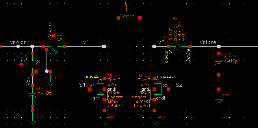
1- Circuit schematic design & simulation
Before everything, you need the right tools or software, also referred as EDA (Electronic Design Automation) software.
Traditionally, Cadence Virtuoso and its ecosystem have been for years the industry standard. However, in the last years other alternatives like Synopsys (very very similar to Cadence) and Siemens EDA (which includes the incredibly popular Calibre tool for physical verification) have become also players in the EDA market.
Designing a circuit is rarely a flat drawing where you just connect resistors, transistors, and capacitors. Instead, circuit design is based on hierarchical structures.
You start at the device level, sizing individual components to build basic cells like current mirrors or differential pairs. These cells are then packaged into larger functional blocks, such as an operational amplifier, regulators or bias generators, which are ultimately connected as symbols at the top level to create the overall system architecture. This modular approach keeps complex designs manageable and reusable.
Moreover, design is a highly iterative process that heavily involves simulation in the loop. You don’t just draw a schematic once, you constantly cycle by tuning your design and running simulations to ensure it will behaves properly in the real world.
2- Layout generation
When fabricating the circuit, each electronic device has a physical structure in the real life. For example, a resistor is a long wire of POLY, a MIM capacitor is two metal layer with an insulator in between. Transistors have a more complex structure with doping regions, metals and poly layers.
All the devices are set together and routed following the schematic connections. Matched transistors or devices need special care and some additional structures have to be added like guard rings or dummies.

3- DRC Check
The “Design Rule Check” is performed often with the tool Calibre, which is fully integrated in Cadence Layout Environment. Calibre is a software from Mentor Grpahics (now Siemens), but there are other alternatives such as Pegasus or Assura.
DRC is a mandatory gatekeeper before a chip can be safely sent to production or “taped out”
In this check, the layout is inspected to comply with the foundry rules and constraints. The DRC scans the layout’s geometric shapes and layers to verify critical parameters, such as the minimum width of metal traces, minimum spacing between adjacent wires, etc , flagging any violations that could lead to short circuits, open circuits, or manufacturing defects.

4- LvS Check
Here the Layout is compared versus the Schematic. The circuit designed in the schematic is compared with the circuit obtained after the layout.
It checks that the connections between components and the dimensions of the components are exactly as drawn in the schematic.
It might seem redundant, but few times the circuits pass LVS on the first run. There are always mismatched parameters or misrouted wires.
The best part of doing Layout is the happy smile obtained after the LVS is completed error-free

5- Antenna and other special rules
After both checks (DRC and LVS) are passed, these manufacturer set of rules ensure that the chip can be fabricated properly without technical problems. I. e. to avoid the so-called “antenna effect”.
Large wires or continuous area of metal connected to transistor gates are not desired, because during the plasma etching fabrication process, the electrostatic charges may destroy the thin-oxide gate dielectric material.
6- Floor Planning
The pads are the connection from the chip to the real world through the wirebonding and the package.
During the floor planing, the electric pads are connected to the designed block, as it can be seen in the picture below. If the chip is composed of various blocks, digital or analog, In this design step, all blocks are connected together.

7- Dummy filling
The standard chip layout rarely utilize 100% of the available area on each metal layer. However, during fabrication, it is important that all layers maintain a relatively uniform material density. Each foundry require a different density rule for each layer and technology node.
Imagine constructing a multi-store building: if a lower floor is mostly empty, it lacks from structural support to the subsequent floors
To fill the empty spaces left on each metal layer, automatic CAD scripts generate all the dummy metal polygons on each layer across the entire layout, while excluding critical regions defined by the designer.


8- Final DRC and LVS Check
While this step might seem redundant if the previous verification stages were performed perfectly, running a final check is a basic industry best practice. Final layout adjustments made late in the design cycle can easily introduce unexpected errors and destroy the entire chip functionality.
In particular, performing a full LVS check after the dummy metal filling has been generated is strongly recommended, because the automatic generation isn’t always error-free. This ensures that the newly added dummy polygons have not accidentally shorted any active nets or introduced parasitic coupling that could alter the circuit’s intended electrical behavior.
9- Export to a GDS file
The final version is finaly exported from Cadence, or other EDA tool. The gds file contains all the polygons and layers that define the transistors, metal routing, vias, and other structures on the chip.
It is straighforward File>> Export >> Stream…

10- Send to the Manufacturer. (“Tape-out”)
In our case, we are part of the EuroPractice. This is a program, launched and supported by the EU, aiming to facilitate the access to chip fabrication, reducing the entrance costs, reducing the risks and giving support.
Once the gds file is exported, we send it to our EuroPractice partner which checks the DRC rules and other aspects again. Usually, they find errors or they suggest some changes. After 2 or 3 iterations. The final gds file is ready.
In our case, the partner EuroPractice, sums up many prototypes into a Multi Project Wafer (MPW) and send it to TSMC, which is the real manufacturer.
At the process, we received an email like this:

11- Receive and test the chip
After some months you will receive a low number of dies. The elapsed time ranges from 2 to 10 months depending on many factors. Between 20 and 40 units to test. You can decide if you want to encapsulate it into a package or not. Packaging a prototype die, it is not really cheap, and could cost almost the same as the fabrication.
For an early stage of prototyping, you may want to only measure the fabricated die on-chip with needles. When you have a more developed prototype, you usually want to include it to a PCB, etc. So in this case, it makes more sense to package.
YOU HAVE A SELF DESIGNED ASIC MICROCHIP


In conclusion, this article provided a concise overview of the analog design flow in ICs, with a focus on the often underestimated layout and intermediate steps.
Each of these steps could be explored in much more detail in separate articles, but the intention here was to offer a brief yet informative description with a helpful flow diagram.
This article aims to contribute to spread and broaden the world of analog IC design and inspire further and new designers.


What did you do next with those dies?
How’s the packaging process?
Hello Navadeep
Yes next steps would be to send for packaging… and then it is ready to use.
On developing processes, you maybe test on wafer (without packaging) because price and time.
Best Regards
There are many steps after Die ready. Packaging is next step.
Die placement/ Monolithic or multi die
BGA ball map design
Routing
plane creation for power
SI/PI
DRC
Tapout
From the Design Flow, why do you think fabrication stage is the most critical?
Hello Lee,
Yes, fabrication is quite critical because it is the most uncontrolled step. On the design, you can control or oversee everything but once the chip is fabricated, it is not easy to know what happened during the fabrication, you can only estimate or estipulate…