A power-on reset for an FPGA is implemented in Verilog and VHDL languages.
Contents
What is a Power-on Reset?
If a synchronous reset is executed at system startup, it is possible that there is no clock signal at this time, since the clock source itself may be subject to a reset. Therefore, the synchronous reset can be ineffective.
Often the Power-On Reset (POR) is generated by an external device, for example, the watchdog, which monitors the supply voltage or the activity of a microprocessor. Then the POR is also not synchronous to the system clock.
Power-on reset (POR) Circuit
It is often used with an RC-circuit in custom ASIC chip designs. In Vivado, there is already a block which provides the functionality: the Xilinx’s Processor System Reset Logic CORE IP.
In this tutorial, a custom POR is implemented with code for any FPGA design.
Proposed POR
The following circuit generates a reset signal from the external POR (in this example low active) which becomes active high for at least 3 clock cycles and then becomes inactive synchronously with the clock. It is crucial that the reset signal is not deactivated within the setup time of a memory, ie shortly before a clock edge!!!
The external POR signal sets the 3 flip-flops of the shift register asynchronous to ‘0’ (= reset). Since it is asynchronous to the system clock, it is called reset_a and is active low.
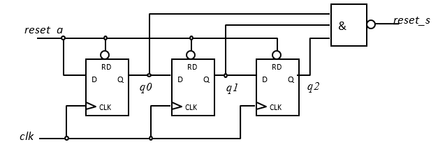
After the POR signal has been deactivated, its inactive value ‘1’ is clocked into the shift register as soon as the system clock is present. The first two flip-flops prevent a possible metastable state from affecting the synchronized reset_s signal, otherwise the entire system would be put into an undefined metastable state.
After 3 clocks all outputs of the 3 flip flops are set to the value ‘1’, which means that the triple NAND gate changes from the value ‘1’ (active reset_s level) to the value ‘0’ (inactive reset_s level ) changes.
Code implementations
Two different way of implementations in Verilog and VHDL languages are here proposed, one with flip-flops and another with shift-registers.
Implementation with FlipFlops in series
Verilog
`timescale 1ns / 1ps
module aufgabe2_1(
      input reset_a,
      input clk,
      output reset_s
);
 reg q0,q1,q2;

//Always beschreibt die 3 FlipFlop Speicherelemente
always@(posedge clk, reset_a)
begin
 if (reset_a == 1'b0)    //reset_a ist asynchron zu clk
 begin
     q0 <= 1'b0;
     q1 <= 1'b0;
     q2 <= 1'b0;
 end
 else if (clk == 1'b1)
 begin
     q0 <= reset_a;
     q1 <= q0;
     q2 <= q1;
 end
end
//nebenläufige kombinatorische Logik
assign reset_s = !(q0 & q1 & q2);
endmodule
VHDL
LIBRARY ieee;
USE ieee.std_logic_1164.all;

entity por is
  port(
    reset_a: in std_logic;
    clk:     in std_logic;
    reset_s: out std_logic
    );
end entity por;

--
architecture rtl of por is
   signal q0,q1,q2: std_logic;
begin
--process beschreibt die 3 FlipFlop Speicherelemente-------
process(clk,reset_a)
begin
   if reset_a = ‘0’ then   -- reset_a ist asynchron zu clk
       q0 <= ‘0’;
       q1 <= ‘0’;
       q2 <= ‘0’;
   elsif clk=’1’ and clk’event then
       q0 <= reset_a;
       q1 <= q0;
       q2 <= q1;
   end if;
end process;

--nebenläufige kombinatorische Logik----
reset_s <= not (q0 and q1 and q2);

end architecture rtl;
The waveform after the simulation looks like:

Implementation with a shift register
Verilog
`timescale 1ns / 1ps
module aufgabe2_1b(
    input reset_a,
    input clk,
    output reset_s
    );
	reg [3:0] q;
always@(posedge clk,reset_a) //auch reset_a muss in der Sensitivity-Liste stehen!!!
begin
//process beschreibt die 3 FlipFlop Speicherelemente
begin
   if(reset_a == 1'b0)	//reset_a ist asynchron zu clk
       q <= 3'b000; //alle Elemente des Vektors q auf '0' setzen
   else if( clk == 1'b1)
       q  <= {reset_a , q[2:1]}; //Schieberegister, rechts schiebend
   end
end
//nebenläufige kombinatorische Logik
assign reset_s = (q == 3'b111) ? 1'b0 : 1'b1;
endmodule
VHDL
LIBRARY ieee;
USE ieee.std_logic_1164.all;

entity por is
  port(
    reset_a: in std_logic;
    clk:     in std_logic;
    reset_s: out std_logic
    );
end entity por;

--
architecture rtl of por is
   signal q: std_logic_vector(2 downto 0);
begin
--process beschreibt die 3 FlipFlop Speicherelemente-------
process(clk,reset_a) -– auch reset_a muss in der Sensitivity-Liste stehen!!!
begin
   if reset_a = ‘0’ then   -- reset_a ist asynchron zu clk
       q <= (others => ‘0’); -- alle Elemente des Vektors q auf ‘0’ setzen
   elsif clk=’1’ and clk’event then
       q  <= reset_a & q(2 downto 1); --Schieberegister, rechts schiebend
   end if;
end process;

--nebenläufige kombinatorische Logik----
reset_s <= ‘0’ when q = “111” else ‘1’;

end architecture rtl;
Simulating this shift register, we would obtain something similar to the next waveform diagram