How to generate a high-frequency PWM signal with an FPGA (Zybo) writing a custom IP in Vivado.
In this article, I am going to explain how to implement a high-speed Pulse Width Modulation (PWM) signal on an FPGA. I made a study comparing several (10) PWM modules with different features and how fast each module can be run.
All the VHDL codes can be found here, as well the Vivado wave simulation, speed consideration and so on. If you have any question, do not hesitate to comment below!
Let’s start!!

Goal
The aim of this project is to develop the fastest possible PWM generator IP block using the Zynq FPGA and VHDL programming language. Pushing to the Limits of the ZYBO to create the fastest PWM possible in VHDL.
Therefore, the constraints are studied to know which are the speed limitations.
For this study, the board utilized is the Zybo from Xilinx. Family of Zynq-7000 FPGAs.
Several versions are developed with different features and configurable parameters.
Maximal theoretical speeds by Zynq-7000
This FPGA incorporates the chip Zynq XC7Z010 which could run up to 464MHz (speed grade -1), according to the datasheet of the XC7Z010 device. Another devices of this Zynq-7010 family can run faster up to 628 MHz (speed grade -3).
Taking this into account, a maximal theoretical speed can be calculated in function of the resolution of the PWM, also the number of bits of the counter.
The bits of resolution is the most limiting factor
Therefore, the next Table 1 shows the maximum theoretical frequency achievable by the PWM module.

For the developing a lower clock frequency is employed. For simplicity, 400 MHz (and 600MHz for speed grade -3) is taken as standard clock speed in all the test in this document if the clock frequency is not detailed. This is due all versions of the PWM cannot run at the highest speed and for comparing purposes a lower clock frequency is used.

PWM Design diagram
The Vivado tool is based on block diagrams, where the system is prepared to be load into the target board.
For synthesis, implementation and bitstream generation, the design from the block diagram of the Figure 2 was employed. This diagram is kept as simple as possible, in order to get the greatest performance of the chip.
The Zynq-processing system core (PS-core) is used as a clock source and it only provides the clock signal to the FPGA. All other peripherals are deactivated. This core can give a maximum of 250 MHz, therefore the clock output of the processor core is set to 200MHz and the clocking wizard is in charge of getting faster clock speeds.

The simulation Test Bench
Simulations are performed to test how the modules behave and to debug possible bugs using the internal signal waves.
Thus, a separated simulation test bench-diagram was used, where all the modules can be tested independently. Here, the clock generator source at 200MHz simulates the clock coming from the PS-core. The desired speed is obtained with the clock wizard block, following the same procedure as in the previous commented FPGA implementation design.

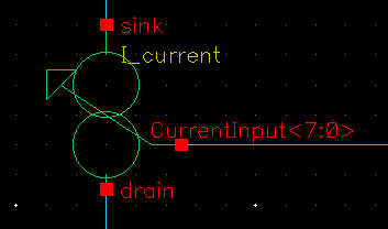
An external RTL module was used to generate the stimuli to simulate several cases for the input values and evaluate the response of the PWM module. The stimuli block generates two signals: Duty cycle as an 8-bits output and a digital enable signal. The full VHDL code of the stimuli block can be found below and the output signals can be seen at the Figure 4.
----------------------------------------------------
-- Constrains file for Zybo PWM FAST project --
-- June 2017 www.AlbertoLopez.eu  --
-- Alberto. L. Gasso alberto@miscircuitos.com --
----------------------------------------------------
library IEEE;
use IEEE.STD_LOGIC_1164.ALL;
use IEEE.std_logic_unsigned.ALL;

entity Stimuli is
	Port (
		Duty_out : out STD_LOGIC_VECTOR (7 downto 0);
		Enable_out : out STD_LOGIC
	);
end Stimuli;

architecture Behavioral of Stimuli is
begin
	STIMULUS: process
		begin
		Duty_out <= "00000000";
		Enable_out <= '0';
		wait for 250 ns;
		Duty_out <= "00001000";
		Enable_out <= '1';
		wait for 800 ns;
		Duty_out <= "11000000";
		wait for 300 ns;
		Duty_out <= "01100000";
		wait for 100ns;
		Enable_out <= '0';
		wait for 654 ns;
		Duty_out <= "10010000";
		wait for 654 ns;
		Duty_out <= "00010000";
		wait for 300 ns;
		Enable_out <= '1';
		wait for 950 ns;
		Duty_out <= "11001000";
		Enable_out <= '0';
		wait for 800 ns;
		Duty_out <= "01000000";
		Enable_out <= '1';
		wait for 654 ns;
		Enable_out <= '1';
		wait; -- end of test
	end process STIMULUS;
end Behavioral;
Module versions
The idea of making different versions is to create polyvalent PWM modules giving to the designer the possibility to choose between a trade of features and speed.
For example in a particular project, only speed could be needed, but the resolution or interlock delay time are not so determinant factors, or vice versa.
In total, 10 versions are developed and studied. Each of them with distinctive features to get the best trade of speed-features.
Common basic features which all PWM module should fulfil:
- Double output: normal and inverted.
- Output should be driven to the pins
- Running at the programable logic (PL) part of the Zynq device.
These variable features are:
- Number of bits of resolution: 4, 6 or 8 bits
- Fixed or variable duty cycle as an input
- Output enable as an input with configurable idle state
- Configurable interlock delay time
- Maximum and minimum saturation limits for the duty cycle
- Synchronized output
The features that should fulfil each version are summarized in the Table 5:

How are the PWM modules tested and compared?
Performance
All the modules were analyzed in terms of timing inside a testbench-diagram created for loading to the FPGA. This diagram has a minimalist design containing only the basic things necessary for running the applications modules.
The clock speed entering to the module was standardized to 400 MHz. Later considering the results given by the 400MHz test, each module was implemented at the maximal runnable speed for the module, which can be higher or lower.
The standard synthesis and implementation strategies for the testbench were determined after the previously mentioned Synsthesis&implementation multivariable test. Therefore, the best strategies for this case are:
- Synthesis: Flow Performance Threshold Carry
- Implementation: Flow Run Post Route Physically Optimized
Versions
Version 1: PWM01
This is the minimal version of a PWM module, the main and only characteristic is:
- Fixed duty cycle by a generic parameter
entity pwm01D is
	generic ( DUTY : integer := 76 ); --default value is 76 = 30%
	Port ( clk : in STD_LOGIC;
			pwm : out STD_LOGIC;
			pwm_i : out STD_LOGIC
		);
end pwm01D;

architecture Behavioral01D of pwm01D is
	signal counter : std_logic_vector(7 downto 0) := "00000000";
	signal pwm_signal : std_logic;
begin
process(clk)
	begin
		if rising_edge(clk) then
			counter <= counter + 1;
		end if;
	end process;

pwm <= '1' when counter > DUTY else '0';
pwm_i <= '0' when counter > DUTY else '1';
end Behavioral01D;
This code generates a simple PWM signal, as it can be seen in the Figure 7. The 8 bit counter rise up to 255, while the duty cycle is fixed at 76 clock cycles (or 29,8%).

To compile this VHDL block and create a functional bitstream to load to the board, the FPGA diagram was used.
The results after running the synthesis and implementation are favourable: 678 picoseconds of positive slack.

This positive result makes possible to increase the clock speed until the maximum supported by the board. Therefore, a new synthesis and implementation with the clock source at 464MHz was performed obtaining 235 picoseconds of positive slack (Figure 9). This would generate a 1.8196 MHz PWM signal with 8-bits resolution.

This positive slack at the maximum FPGA clock speed shows that the limitation factor for this module is the FPGA itself. In this case, if another FPGA with a higher speed grade is used, higher speed can be achieved.
A synthesis and implementation with the Zynq chip XC7Z020 were done. This allows to test how fast could be the speed grade -3, the fastest device available of this Chip-family. The result was a positive slack with 628 MHz clock, generating theoretically a 2.4627 MHz PWM signal.

Version 2: PWM02
This PWM module adds new features:
- (new) Duty cycle as input
- (new) The duty cycle only changes at the end of the cycle

The duty cycle for the PWM signal comes from an external pin. This approach is based on the previous version, but adding the input value. The duty cycle value should be only refreshed at the beginning of each cycle. The following VHDL code was written:
entity pwm02 is
	Port ( clk : in STD_LOGIC;
		duty : in STD_LOGIC_VECTOR (7 downto 0);
		pwm : out STD_LOGIC;
		pwm_i : out STD_LOGIC
	);
end pwm02;

architecture Behavioral02 of pwm02 is
	signal counter : std_logic_vector (7 downto 0) := "00000000"; --initialize to 0
	signal duty_sig : std_logic_vector (7 downto 0) := "00000000";
	begin
	process(clk)
	begin
		if rising_edge(clk) then
			counter <= counter + 1;
		end if;
		if counter = 0 then
			duty_sig <= duty;
		end if;
	end process;
pwm <= '1' when counter <= duty_sig else '0';
pwm_i <= '1' when counter < duty_sig else '0';
end Behavioral02;
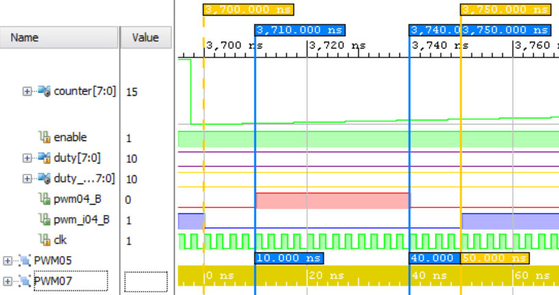
The simulation of PWM 02 block was made applying the stimuli signal described before in Figure 4, the following output signal is obtained (Figure 12). The gold duty signal is read from the stimuli, it is the input.
The green duty_sig wave is the actualized value. It can be seen that this actual duty cycle value (green duty_sig) is only at the end of every counter cycle refreshed. For example in the Figure 12 at the time ~ 1.1ns, the duty = 0xC8 is not taken in account because the 0x60 value was the value at the end of the cycle.

After the synthesis and implementation of this PWM module a positive slack of 753 picoseconds is gotten.

This module has enough positive slack to run at the maximum speed (464MHz). For this synthesis and implementation also a positive slack is obtained, as it can be seen on the Figure 14.

Version 3: PWM03
This module inherits some features from the previous one and adds an enable input.
The features for the third version are:
- Duty cycle as input.
- The duty cycle only changes at the end of the cycle.
- (new) Enable input. If disabled, the outputs of the PWM should be switched to its idle state.
For this module a function was created to convert the Boolean generic parameter into std_logic format.
entity pwm03 is
	generic( IDLE : boolean := false;
			IDLE_I: boolean := false
			);
	Port ( clk : in STD_LOGIC;
		duty : in STD_LOGIC_VECTOR (7 downto 0);
		enable : in STD_LOGIC;
		pwm : out STD_LOGIC;
		pwm_i : out STD_LOGIC
	);
end pwm03;

architecture Behavioral03 of pwm03 is
	signal counter : std_logic_vector (7 downto 0) := "00000000"; signal duty_sig : std_logic_vector (7 downto 0) := "00000000";

function bool_to_sl(X : boolean)--conversion from boolean to std_logic
	return std_ulogic is
	begin
		if X then
			return '1';
		else
			return '0';
		end if;
	end BOOL_TO_SL;

begin
process(clk)
	begin
	if rising_edge(clk) then
		if enable = '1' then
			counter <= counter + 1;
			if counter <= duty_sig then
				pwm <= '0';
				pwm_i <= '1';
			else
				pwm <= '1';
				pwm_i <= '0';
			end if;
		else --Enable = '0'
			counter <= (others => '0');
			pwm <= bool_to_sl(IDLE);
			pwm_i <= bool_to_sl(IDLE_I);
		end if;
	end if;
	--update the dutycycle only at the end of each PWM-cycle
	if counter = 0 then
		duty_sig <= duty;
	end if;
end process;
end Behavioral03;
The functionality of this enable input is shown in the Figure 16. The idle state for the simulation was set to zero for both signals. This can be changed by double clicking on the instantiated block and checking the variable box of the Figure 15.


This module after synthesis and implementation has a positive slack at 400 MHz clock speed of 445 picoseconds

Version 4: PWM04
This fourth version is the first functional stable module and usable by a power electronics bridge.
The features are the following:
- Duty cycle as input.
- The duty cycle only changes at the end of the cycle.
- Enable input. If disabled, the outputs of the PWM should be switched to its idle state.
- 8 bits resolution.
- (new) Fixed interlock by generic parameter.
entity pwm04B is
generic(    IDLE  : boolean := false;
            IDLE_I: boolean := false;
            INTERLOCK :integer := 4
            );
    Port ( clk : in STD_LOGIC;
           duty : in STD_LOGIC_VECTOR (7 downto 0);
           enable : in STD_LOGIC;
           pwm : out STD_LOGIC;
           pwm_i : out STD_LOGIC
           );
end pwm04B;

architecture Behavioral04B of pwm04B is
    signal counter : std_logic_vector(7 downto 0) := "00000000";
    signal duty_sig : std_logic_vector (7 downto 0) := "00000000";
    signal duty_sig_i : std_logic_vector (7 downto 0) := "00000000";

function bool_to_sl(X : boolean)--conversion from boolean to std_logic
              return std_ulogic is
    begin
      if X then
        return '1';
      else
        return '0';
      end if;
end BOOL_TO_SL;
begin
process(clk)
        begin
        if rising_edge(clk) then
            if enable = '1' then
                counter <= counter + 1; --pwm signal with interlock delay time if counter >= INTERLOCK and counter < duty_sig then
                    pwm <= '1';
                else
                    pwm <= '0'; end if; --inverted pwm signal if counter >= duty_sig_i  then
                   pwm_i <= '1';
                else
                   pwm_i <= '0';
                end if;
            else --enable = '0'
                counter <= (others => '0');
                pwm   <= bool_to_sl(IDLE); --Set to iddle state
                pwm_i <= bool_to_sl(IDLE_I);  --Set to iddle state
            end if;
        end if;
--update the dutycycle only at the end of each PWM-cycle
        if counter = 0 then
            duty_sig <= duty ;
            duty_sig_i <= duty+ INTERLOCK;
        end if;
end process;
end Behavioral04B;
Code 3: Extract from PWM 04 module
The simulations wave for this module can be seen at the Figure 18, where the interlock delay of 4 clock cycles can be appreciated. The interlock delay time is equally divided between the normal and inverted signal.
The duty cycle can be calculated as following:
Where duty and interlock are measured in clock cycles.

The duty cycle calculation can be done after the simulation signals:

The synthesis and implementation for this PWM module at 400 MHz the module returns a positive slack of 120 picoseconds (Figure 20).

This module can run at 450MHz clock speed creating a 1,75 MHz PWM signal

The output signal of this module on the oscilloscope can be seen in the next Figure 22:
The signal shown above can not be well displayed because the measurement equipment is not fast enough. The speed of the used oscilloscope is 100GHz. This lead on bad edges on the transitions.
Alternative: PWM05
For this functional fourth version, another coding option with identical functionality were tested. In this module, the use of an external counter block was implemented in the PWM05, as it can be seen on the Figure 23. This could be beneficious when more module in parallel share a common external counter.

After the synthesis and implementation, it was concluded that the use of an external counter is slower, in terms of maximum clock frequency, than using a user defined VHDL counter with a std_logic_vector signal. The synthesis and implementation finished with only 48 picoseconds of slack (Figure 24).
Version 5: PWM06
Features of this module:
- Duty cycle as input.
- The duty cycle only changes at the end of the cycle.
- Enable input. If disabled, the outputs of the PWM should be switched to its idle state.
- 8-bits resolution.
- Interlock as input (new)
----------------------------------------------------
-- Constrains file for Zybo PWM FAST project      --
-- June 2017 FH-Joanneum                          --
-- Alberto. L. Gasso alberto@miscircuitos.com          --
----------------------------------------------------
library IEEE;
use IEEE.STD_LOGIC_1164.ALL;
use IEEE.std_logic_unsigned.ALL;

entity pwm06 is
generic(    idle  : boolean := false;
            idle_i: boolean := false
            );
    Port ( clk : in STD_LOGIC;
           duty : in STD_LOGIC_VECTOR (7 downto 0);
           enable : in STD_LOGIC;
           interlock : STD_LOGIC_VECTOR(3 downto 0);
           pwm : out STD_LOGIC;
           pwm_i : out STD_LOGIC
           );
end pwm06;

architecture Behavioral06 of pwm06 is
    signal counter : std_logic_vector(7 downto 0) := "00000000";
    signal duty_sig : std_logic_vector (7 downto 0) := "00000000";
    signal duty_sig_i : std_logic_vector (7 downto 0) := "00000000";

function bool_to_sl(X : boolean)--conversion from boolean to std_logic
              return std_ulogic is
    begin
      if X then
        return '1';
      else
        return '0';
      end if;
end BOOL_TO_SL;

begin
process(clk)
        begin
        if rising_edge(clk) then
            if enable = '1' then
                counter <= counter + 1; --pwm signal with interlock delay time if counter >= interlock and counter < duty_sig then
                    pwm <= '1';
                else
                    pwm <= '0'; end if; --inverted pwm signal if counter >= duty_sig_i then
                   pwm_i <= '1';
                else
                   pwm_i <= '0';
                end if;
            else --enable = '0'
                counter <= (others => '0');
                pwm   <= bool_to_sl(IDLE); --Set to iddle state
                pwm_i <= bool_to_sl(IDLE_I);  --Set to iddle state
            end if;
        end if;
--update the dutycycle only at the end of each PWM-cycle
        if counter = 0 then
            duty_sig <= duty;
            duty_sig_i <= duty + interlock;
        end if;
end process;
end Behavioral06;
After the synthesis and implementation at 400 MHz a positive slack was obtained, as it can be seen at Figure 26. but compared with the previous version 4, it is slower.

This feature is not really needed in real applications for power electronics. The interlock delay time varies between different systems, where it can be better fixed by a generic parameter for each system.
Version 6: PWM07
This new module is based on the PWM04. Features of this module:
- Duty cycle as input.
- The duty cycle only changes at the end of the cycle.
- Enable input. If disabled, the outputs of the PWM should be switched to its idle state.
- 8-bits resolution.
- (new) Fixed interlock by generic parameter.
- (new) Variable saturation limits for the duty cycle by generic parameter
This limitation is based on many power devices cannot handle 100% duty cycle, and they have some security control implemented. When the controller has this feature, the power electronics device can dispense with this. For this function, the following Code 4 was added into
----------------------------------------------------
-- Constrains file for Zybo PWM FAST project      --
-- June 2017 FH-Joanneum                          --
-- Alberto. L. Gasso alberto@miscircuitos.com          --
----------------------------------------------------
library IEEE;
use IEEE.STD_LOGIC_1164.ALL;
use IEEE.std_logic_unsigned.ALL;

entity pwm07 is
generic(    IDLE  : boolean := false;
            IDLE_I: boolean := false;
            INTERLOCK :integer := 4;
            MAX_DUTY : STD_LOGIC_VECTOR (7 downto 0 ) := "11110101"; --245
            MIN_DUTY : STD_LOGIC_VECTOR (7 downto 0 ) := "00010100"  --20
            );
    Port ( clk : in STD_LOGIC;
           duty : in STD_LOGIC_VECTOR (7 downto 0);
           enable : in STD_LOGIC;
           pwm : out STD_LOGIC;
           pwm_i : out STD_LOGIC
           );
end pwm07;

architecture Behavioral07 of pwm07 is
    signal counter : std_logic_vector(7 downto 0) := "00000000";
    signal duty_sig : std_logic_vector (7 downto 0) := "00000000";
    signal duty_sig_i : std_logic_vector (7 downto 0) := "00000000";
function bool_to_sl(X : boolean)--conversion from boolean to std_logic
                  return std_ulogic is
        begin
          if X then
            return '1';
          else
            return '0';
          end if;
    end BOOL_TO_SL;
begin
process(clk)
        begin
        if rising_edge(clk) then
            if enable = '1' then
                counter <= counter + 1; --pwm signal with interlock delay time if counter >= INTERLOCK and counter < duty_sig then
                    pwm <= '1';
                else
                    pwm <= '0'; end if; --inverted pwm signal if counter >= duty_sig_i then
                   pwm_i <= '1';
                else
                   pwm_i <= '0';
                end if;
            else --enable = '0'
                counter <= (others => '0');
                pwm   <= bool_to_sl(IDLE); --Set to iddle state
                pwm_i <= bool_to_sl(IDLE_I); --Set to iddle state end if; end if; --update the dutycycle only at the end of each PWM-cycle if counter = 0 then if duty > MAX_DUTY then
                duty_sig <= MAX_DUTY;
                duty_sig_i <=MAX_DUTY + INTERLOCK;
            elsif duty< MIN_DUTY then
                duty_sig <= MIN_DUTY;
                duty_sig_i <=MIN_DUTY + INTERLOCK;
            else
                duty_sig <= duty;
                duty_sig_i <=duty + INTERLOCK;
            end if;
        end if;
end process;
end Behavioral07;
Code 4: Extract PWM 07
Simulating the PWM block with the following parameters:


As it can be seen on the Figure 27, the input signal of duty (in purple) is limited at time 3µs by the minimum limit. It takes the minimum value 0x14 instead of the given value of 0x10. On the other hand, at time 5µs, it saturates to 0xF4 instead of the given duty signal of 0xFF.
The Slack is positive,251 picoseconds, for this module can be found at the Figure 29.

Version 7: PWM08
Features of this module:
- Duty cycle as input.
- The duty cycle only changes at the end of the cycle.
- Enable input. If disabled, the outputs of the PWM should be switched to its idle state.
- Fixed interlock by generic parameter
- Variable saturation limits for the duty cycle by generic parameter
- (new) Starting value of the counter adjustable by a generic parameter.
----------------------------------------------------
-- Constrains file for Zybo PWM FAST project      --
-- June 2017 FH-Joanneum                          --
-- Alberto. L. Gasso alberto@miscircuitos.com          --
----------------------------------------------------
library IEEE;
use IEEE.STD_LOGIC_1164.ALL;
use IEEE.std_logic_unsigned.ALL;
use IEEE.std_logic_arith.all;

entity pwm08 is
generic(    IDLE  : boolean := false;
            IDLE_I: boolean := false;
            INTERLOCK :integer := 4;
            MAX_DUTY : integer  := 245; --245 "11110101"
            MIN_DUTY : integer := 20;  --20 "00010100"
            START : integer := 127     --x"7F"
            );
    Port ( clk : in STD_LOGIC;
           duty : in STD_LOGIC_VECTOR (7 downto 0);
           enable : in STD_LOGIC;
           pwm : out STD_LOGIC;
           pwm_i : out STD_LOGIC
           );
end pwm08;

architecture Behavioral08 of pwm08 is
    signal counter : STD_LOGIC_VECTOR (7 downto 0) :=  CONV_STD_LOGIC_VECTOR(START,8);
    signal duty_sig : integer range 0 to 255 := 0;
    signal duty_sig_i : integer range 0 to 255 := 0;

function bool_to_sl(X : boolean)--conversion from boolean to std_logic
              return std_ulogic is
    begin
      if X then
        return '1';
      else
        return '0';
      end if;
end BOOL_TO_SL;
begin
process(clk)
        begin
        if rising_edge(clk) then
            if enable = '1' then
                counter <= counter + 1; --pwm signal with interlock delay time if counter >= INTERLOCK and counter < duty_sig then
                    pwm <= '1';
                else
                    pwm <= '0'; end if; --inverted pwm signal if counter >= duty_sig_i  then
                   pwm_i <= '1';
                else
                   pwm_i <= '0';
                end if;
            else --enable = '0'
                counter <= CONV_STD_LOGIC_VECTOR(START,8);
                pwm   <= bool_to_sl(IDLE);  --Set to iddle state
                pwm_i <= bool_to_sl(IDLE_I); --Set to iddle state end if; end if; --update the dutycycle only at the end of each PWM-cycle if counter = 0 then if duty > MAX_DUTY then
                duty_sig <= MAX_DUTY;
                duty_sig_i <=MAX_DUTY + INTERLOCK;
            elsif duty< MIN_DUTY then
                duty_sig <= MIN_DUTY;
                duty_sig_i <=MIN_DUTY + INTERLOCK;
            else
                duty_sig <= CONV_INTEGER( duty);
                duty_sig_i <=CONV_INTEGER(duty)+ INTERLOCK;
            end if;
        end if;
end process;
end Behavioral08;

This implementation leads to the possibility of creating many PWM modules interleaved with different phase. This can be seen on the Figure 32, that the counter starts at 127 after the enable signal is set. Also, the saturation limits for the duty cycle are active in this module, as shown in the previous one.

The results of the synthesis and implementation for this module is 127 picoseconds (Figure 33).

Version 8: PWM09
For this module, a synchronization signal is added to manage the use of multiple PWM modules in separated boards. This avoid the possible clock deviation when multiple boards are being used.
Features of this module:
- Duty cycle as input.
- The duty cycle only changes at the end of the cycle.
- Enable input. If disabled, the outputs of the PWM should be switched to its idle state.
- Fixed interlock by generic parameter
- Variable saturation limits for the duty cycle by generic parameter
- Starting value of the counter adjustable by a generic parameter
- Synchronization signal (new)
----------------------------------------------------
-- Constrains file for Zybo PWM FAST project      --
-- June 2017 FH-Joanneum                          --
-- Alberto. L. Gasso alberto@miscircuitos.com          --
----------------------------------------------------

library IEEE;
use IEEE.STD_LOGIC_1164.ALL;
use IEEE.std_logic_unsigned.ALL;
use IEEE.std_logic_arith.all;

entity pwm09 is
generic(    IDLE  : boolean := false;
            IDLE_I: boolean := false;
            INTERLOCK :integer := 4;
            MAX_DUTY : integer  := 245; --245 "11110101"
            MIN_DUTY : integer := 20;  --20 "00010100"
            START : integer := 127     --x"7F"
            );
    Port ( clk : in STD_LOGIC;
           duty : in STD_LOGIC_VECTOR (7 downto 0);
           enable : in STD_LOGIC;
           sync_in : in STD_LOGIC;
           sync_out : out STD_LOGIC;
           pwm : out STD_LOGIC;
           pwm_i : out STD_LOGIC
           );
end pwm09;

architecture Behavioral09 of pwm09 is
    signal counter : STD_LOGIC_VECTOR (7 downto 0) :=  CONV_STD_LOGIC_VECTOR(START,8);
    signal duty_sig : integer range 0 to 255 := 0;
    signal duty_sig_i : integer range 0 to 255 := 0;

function bool_to_sl(X : boolean)--conversion from boolean to std_logic
              return std_ulogic is
    begin
      if X then
        return '1';
      else
        return '0';
      end if;
end BOOL_TO_SL;

begin
process(clk)
        begin
        if rising_edge(clk) then
            if enable = '1' then
                counter <= counter + 1; --pwm signal with interlock delay time if counter >= INTERLOCK and counter < duty_sig then
                    pwm <= '1';
                else
                    pwm <= '0'; end if; --inverted pwm signal if counter >= duty_sig_i then
                   pwm_i <= '1';
                else
                   pwm_i <= '0';
                end if;
            else --enable = '0'
                counter <= CONV_STD_LOGIC_VECTOR(START,8);
                pwm   <= bool_to_sl(IDLE);  --Set to iddle state
                pwm_i <= bool_to_sl(IDLE_I);  --Set to iddle state
            end if;
            sync_out <= '0'; --For Master synchronization
            if sync_in = '1' then
                 counter <= CONV_STD_LOGIC_VECTOR(START,8)+1; end if; end if; --update the dutycycle only at the end of each PWM-cycle if counter = 0 then if duty > MAX_DUTY then
                duty_sig <= MAX_DUTY;
                duty_sig_i <=MAX_DUTY + INTERLOCK;
            elsif duty< MIN_DUTY then
                duty_sig <= MIN_DUTY;
                duty_sig_i <=MIN_DUTY + INTERLOCK;
            else
                duty_sig <= CONV_INTEGER( duty);
                duty_sig_i <=CONV_INTEGER(duty)+ INTERLOCK;
            end if;
            --For Master output
            sync_out <= '1';
        end if;
end process;
end Behavioral09;
For this synchronized design, an unique master role is needed to provide the tick to the slave modules. In normal conditions, slaves which are running in the same board as the master, they should never desynchronize with the master, but to be in the safe region, and to run all slaves the same conditions, the master output synchronization signal is returned to as an input for the inboard slaves.
Two different modules were created for this version: Master and slave.

In the simulation environment, to test the synchronization of modules running in separated boards, two clock sources are used. One for the master at 400MHz and another slightly higher for some slaves at 401MHz. This should lead to asynchronous PWM signal of the three interleaved pwm modules.
For the test two slaves and one master are instanciated. After 70.000ns the signals are not any more synchronized. The simulations diagram can be seen on the Figure 35.

In the slave 0 of the Figure 36 can be seen that the phase is totally out after 80 µs of simulation.

To avoid the possible asynchronization between different boards, the sync-signal provide a high pulse when the period starts. This makes the system dynamically synchronize, while the PWM is being generated. The diagram with the sync signal in green can be seen at the Figure 37. The following Figure 38 shows that the system is not affected with the clock deviation of the slave modules.


To test how fast can be synthetized and implemented the following block diagram (Figure 39) was built.


Version 9: PWM10
This is the last and most complete version. The PWM 10 module is identical as the previous version 9, but it allows you to vary the resolution of bits.
The features of the module:
- Duty cycle as input.
- The duty cycle only changes at the end of the cycle.
- Enable input. If disabled, the outputs of the PWM should be switched to its idle state.
- Fixed interlock by generic parameter
- Variable saturation limits for the duty cycle by generic parameter
- Starting value of the counter adjustable by a generic parameter
- Synchronization signal
- (new) Generic number of bit of resolution
This version has been solved by the previous version 9: one master gives the synchronization signal and the slaves generate the PWM. The master block remains equal as before, but the slave module incorporates a generic parameter of number of bits. By this generic parameter, the length of the counter is changed and therefore the PWM signal resolution.
----------------------------------------------------
-- Constrains file for Zybo PWM FAST project      --
-- June 2017 FH-Joanneum                          --
-- Alberto. L. Gasso alberto@miscircuitos.com          --
----------------------------------------------------
library IEEE;
use IEEE.STD_LOGIC_1164.ALL;
use IEEE.std_logic_unsigned.ALL;
use IEEE.std_logic_arith.all;

entity pwm10S is
generic(    BITS : integer := 8;    --number of bit of cresolution
            IDLE  : boolean := false;   --idle state for pwm signal
            IDLE_I: boolean := false;   --idel state for pwm inverted signal
            INTERLOCK :integer := 4;    --number of cycles for the interlock delay time
            MAX_DUTY : integer  := 245; --245 "11110101"
            MIN_DUTY : integer := 20;  --20 "00010100"
            START : integer := 127     --x"7F"
            );
    Port ( clk : in STD_LOGIC;
           duty : in STD_LOGIC_VECTOR (BITS-1 downto 0);
           enable : in STD_LOGIC;
           sync_in : in STD_LOGIC;
           pwm : out STD_LOGIC;
           pwm_i : out STD_LOGIC
           );
end pwm10S;

architecture Behavioral10S of pwm10S is
    signal counter : STD_LOGIC_VECTOR (BITS-1 downto 0) :=  CONV_STD_LOGIC_VECTOR(START,BITS);
    signal duty_sig : integer range 0 to 1024 := 0;
    signal duty_sig_i : integer range 0 to 1024 := 0;
    signal sync_inDel : std_logic; --to store the synchronization signal value


function bool_to_sl(X : boolean)--conversion from boolean to std_logic
              return std_ulogic is
    begin
      if X then
        return '1';
      else
        return '0';
      end if;
end BOOL_TO_SL;

begin

process(clk)
        begin
        if rising_edge(clk) then
            if enable = '1' then
                counter <= counter + 1; --pwm signal with interlock delay time if counter >= INTERLOCK and counter < duty_sig then
                    pwm <= '1';
                else
                    pwm <= '0'; end if; --inverted pwm signal if counter >= duty_sig_i then
                   pwm_i <= '1';
                else
                   pwm_i <= '0';
                end if;
            else --enable = '0'
                counter <= CONV_STD_LOGIC_VECTOR(START,BITS);
                pwm   <= bool_to_sl(IDLE);  --Set to iddle state
                pwm_i <= bool_to_sl(IDLE_I);  --Set to iddle state
            end if;
        end if;
        --Read the synchronization signal
        if (sync_in = '1' and sync_inDel = '0') or (sync_in = '0' and sync_inDel = '1')then
            counter <= CONV_STD_LOGIC_VECTOR(START,BITS)+1;
        end if;
        sync_inDel <= sync_in; --update the dutycycle only at the end of each PWM-cycle if counter = 0 then if duty > MAX_DUTY then
                duty_sig <= MAX_DUTY;
                duty_sig_i <=MAX_DUTY + INTERLOCK;
            elsif duty< MIN_DUTY then
                duty_sig <= MIN_DUTY;
                duty_sig_i <=MIN_DUTY + INTERLOCK;
            else
                duty_sig <= CONV_INTEGER( duty);
                duty_sig_i <=CONV_INTEGER(duty)+ INTERLOCK;
            end if;
        end if;
end process;
end Behavioral10S;
The test for this module to get the maximum performance with one module at 400. Below can be seen the diagram used for the test and in the


A small application of multiphase pwm is done here with three interleaved at 120° resulting a positive slack of 55 picoseconds:

The special feature of this module is the possibility of varying the values of the resolution easily from the generic block properties. The PWM frequency can be changed without comprising the slack time. The Worst Negative Slack depends on how many modules in parallel are placed on the Table 7:

To choose a certain PWM frequency speed, the most suitable procedure without losing resolution is to set first the number of resolution bits depending on the maximal frequency. Then down the clock speed.
For example, if 2 MHz PWM speed is required:
Looking at the Table 7, to get 2 MHz is possible only with maximal of 7 bits resolution. Then the new clock speed should be calculated.


Hi Alberto,
thanks for your tutorial it was really helpfull for me. Im using an spartan-6 with ISE 14.7 and I want to use a full bridge with the pwm. I already implemented the PWM (Im able to send TBPRD, ENABLE) but I want to be able to generate an interrupt for the PWM to get 50Hz sine wave.
Im using a sine table of 360 points, Im using 50Mhz clock so I put a counter to count-up to 2777. I genenerate a 18Khz PWM with no problems. But the interrupt is generate each time the counter reach the 2777 value. And looking the scope I always get 1Hz output sinewave. How can I be able to generate 50Hz sinewave ouput?
Thank you, this is excellent!