IC thyristor-based oscillators offer an ultra-low-power consumption clock alternative for applications where accuracy isn’t important and a low frequency is required.
In this short tutorial, we are going to simulate and test a thyristor-based ring oscillator using Cadence Virtuoso, presenting the schematic diagrams and simulation plots.
Let’s start from the beginning
What is a Thyristor?
A thyristor is a type of semiconductor device that acts like a switch and has 3 terminals: Anode (A), Cathode (K) and Gate (G).
Its functionality is similar to transistors, but with the difference that when it is triggered with a high voltage at the gate, it remains ON (conducting) even if the gate control signal is removed. The thyristor remains ON forever theoretically. However… due to leak currents, after some time has elapsed, it flips and turns off (non-conducting). This property is exploited in this case for our benefit.
The thyristor can be considered as a one-way transistor

Thyristor Ring Oscillator
A thyristor ring oscillator works identically to an inverter-based ring oscillator. Interestingly, ring oscillators were first presented in 1995 in the Solid-State Circuit Journal. [1]
A cascaded odd number of inverters connected in a closed loop
For this ring design example, I will use 3 elements, which is the minimum number of elements in the chain to obtain oscillations.

Thyristors are used as a latch. The delay of each thyristor-based inverter depends on the leakage current of the CMOS transistor, which discharges the node slowly until the threshold voltage is met and the state switches. Therefore, the delay time is much, much slower than a regular CMOS inverter. Consequently, while ring oscillators generate a clock in the MHz range, thyristor-based oscillators work in the Hz range.
Ring oscillators are in MHz range, while Thyristor-based ring oscillators operate in the Hz range
An enormous advantage is the very low power consumption. The circuit requires only a minimal amount of current during transitions to charge the nodes. Its static power consumption is near to zero.
They oscillate at low frequencies, which is desired for some applications.
Usually, low-frequency clock signals are generated using frequency dividers and high-frequency clock sources. However, the power consumption is very high due to the significant switching activity involved in the process.
The main drawback is the fragile robustness of the system. The fact that the delay, and therefore the output frequency, is proportional to the leakage current makes the circuit unreliable due to excessive uncertainties, which are often unacceptable in commercial IC design.
Leakage current is usually not properly modeled in many technologies. Furthermore, it has a very strong dependency on process parameters and temperature variations. This makes the block’s simulations not accurate compared to the fabricated device.
Schematic Diagram
The schematic of this slow clock is presented on the schematic below:
 Oscillator Start-up
 Oscillator Start-up
A small circuit with a capacitor and 2 transistors is used to force the oscillation at the beginning. One of the challenges of the ring oscillators is ensuring the first cycle of oscillation, avoiding metastability. Once the oscillator is operating, it oscillates indefinetely.
In real life, for a fabricated silicon integrated circuit with a ring oscillator, it is rare for it to remain in a metastable position. This is due to impurities and the fact that not all the transistors are not perfectly 100% identical, the oscillation will be naturally provoked.
In simulation, the transistors are ideally identical, with the same exact modeled behavior. This causes metastability in simulations. However, in IC design, robustness is critical and strongly important. All the uncertainties are highly undesired and always avoided.
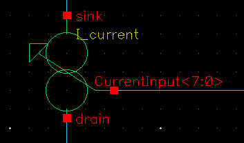
A CMOS Thyristor Block
Several CMOS structures can be used to emulate the behavior of a thyristor. The chosen architecture for this example is a CMOS thyristor with footer transistors because of the low power consumption [2].
This block is a differential Thyristor with 2 complementary inputs (R) and outputs (Q).

Output Stage
At the output of the ring, there is an interface stage designed to convert the oscillation waveform into a well-defined signal with sharper transitions and a full voltage swing. Typically, it consists of an inverter chain to reduce the rise and fall times, provide more driving strength and isolate (buffering) the ring from the external circuits.
This stage must be adapted and designed for each application.
Cadence Simulations
To simulate and test the block, the oscillator is encapsulated in a symbol, as shown in the pic below. The test bench is quite simple: a supply voltage (VAUX = 1.2V) and a connection to the global ground (gnd!).

The functionality is checked with a simple transient analysis. The waveform has unbalanced but squared and regular oscillations. The output is rail-to-rail from 0 to 1.2V.

The average current consumption of the oscillator is only 1.9nA for a frequency of 43 Hz. We can calculate the Figure of Merit (FoM) of the oscillator by dividing the current consumption by the frequecy (Ivdd/freq) to determine how many Amperes are needed for each clock cycle. The FoM is 0.044nA/Hz.

The startup circuit functionality can be seen on the following wave diagram:

The Output signal and the inner signals are displayed on the next simulation diagram. It can be seen how the output stage cleans the inner signals.

Frequency adjustment
This is only an example, the frequency must be modified to match the specifications of each application.
Both capacitor sizes determine the capacitance of the node and therefore, how much energy needs to be discharged through the leak. Hence, the capacitance value varies inversely with the frequency.
More capacity — > slower clock — > lower frequency
With a parametric simulation, this relationship can be easily observed. The capacitance is multiplied by the multiplier parameter, which varies among 1, 2, 5, 10, 20 and 50.

The output frequency are different:

Thus, the leak current is proportional to the frequency.
More leak current — > higher frequency
Layout
A good layout is extremely important in circuits like this because they rely on such small capacitances. The stray capacitors from the devices, paths and vias directly modify the behavior of the design, typically lowering down the output frequency. Corners and Monte Carlo simulations are an important step to verify the robustness of these fragile circuits.
Consequently, it is important to run post-layout simulations before the tape out and sending it to fabrication. Nevertheless, as mentioned previously, the leakage currents are not well modeled in the post-layout models either.
Conclusion
Sources
[1]: Gyudong Kim, Min-Kyu Kim, Byoung-Soo Chang and Wonchan Kim, “A low-voltage, low-power CMOS delay element,” in IEEE Journal of Solid-State Circuits, vol. 31, no. 7, pp. 966-971, July 1996, doi: 10.1109/4.508210.
[2]: (extract) Thyristor-based oscillator. Extract of my Thesis with a Monte Carlo analysis of the thyristor type election.
[3]: A. K. Mahato, “Ultra low frequency CMOS ring oscillator design” 2014 Recent Advances in Engineering and Computational Sciences (RAECS), 2014, pp. 1-5, doi: 10.1109/RAECS.2014.6799627.


Hie, Alberto I am new to monte Carlo simulation so can you tell from where I started to learn Monte Carlo simulation from inverter design we start to learn Monte Carlo simulation also tell everything about monte Carlo simulation for eg why we need what parameter we calculate and all other things
Hello Pavan,
Take a look of my Monter Carlo Introduction in Cadence: https://miscircuitos.com/monte-carlo-simulation-cadence-virtuoso/
it may help you.
Best Regards
Alberto
Hello Alberto,
Can a ring oscillator on purpose be made to have more jitter? I would like to use the random jitter to determine if Mental intention can alter its random characteristics.
Hello Dr. Robert,
The jitter is a non-desirable effect, but as we know how to minimize it, you can also deliberately incite it. For example with a bad analog layout of the traces allowing reflection or a slow slew rate.