The Tie Cells are small circuits used to connect (or tie) gates or input logic gates to vdd power or ground.
The aim is to protect the gate of the transistors, avoiding fabrication issues and to maintain signal integrity and robustness.
Tie cells are used to prevent direct connections from VDD or VSS (power supply rails) to the inputs of logic gates.
These cells are often included in a standard cell library provided in the technology.
There are two types: Tie-Low and Tie-High.
But… Why do we need a Tie Cell?
The short answer:
To not break the transistors during the fabrication and for robustness/ signal integrity.
The full answer:
In actual technology nodes, the gate oxide layer under the poly gate in a mosfet is very thin and sensitive. This thin gate oxide is a critical element during both the fabrication process (similar to the antenna effect) and also during the operation time. This careful consideration prevents any damage to the sensitive gate oxide.
If we connect directly the polysilicon gate to VDD or GND for a constant high or low input signal, any sudden surge or glitch in the supply voltage would lead to the deterioration of the delicate gate oxide.
To mitigate the risks mentioned, a general practice is avoiding the direct connection from VDD or VSS to the input of any logic gates.
Summarizing the reasons, the tie cell…
Protect the Gate Oxide
The gate oxide under the gate of transistors is thin and sensitive. This is crucial to protect the thin gate oxide from damage that can occur due to voltage surges or glitches, especially when the polysilicon gate connects directly to power or ground for constant high or low input signals.
Mitigate the antenna effect:
The antenna effect is a well known phenomenon in the semiconductor industry, where charge accumulates on interconnects during the fabrication process, leading to potential damage during fabrication processes.
Signal Integrity and Robustness:
Tie cells contribute to signal integrity by managing the connection of signals to power or ground. By avoiding direct connections and using tie cells strategically, designers can enhance the robustness and reliability of the integrated circuit, particularly in the presence of unexpected events like voltage fluctuations.
Voltage spikes in vdd and gnd are not propagated to the output of the tie cell.
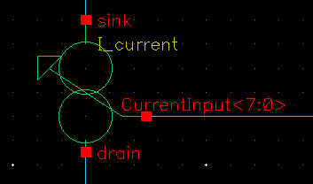
The Tie Cells: CMOS Circuit Implementation
To address the previous mentioned problem, a “tie cell” is employed.
The tie cell allows us to connect the input of any logic gate to VDD or GND with safety, ensuring that the sensitive gate oxide is safeguarded against potential damage caused by voltage surges or glitches.
Schematic
The cells are built with 2 complementary transistors.
The block is supplied with Vdd and gnd and it has only one output, but ANY input.

Analyzing the Tie-high cell, it is a diode-connected nmos attached to the pmos gate.
As the diode is always conducting, it is bringing the pmos gate to a low state, and therefore the pmos is conducting. So, the output of the cell will be always high.
In summary, tie cells are essential components in IC design, serving to connect gates to VDD or ground safely. These small blocks protect the sensitive gate oxide layers, preventing fabrication issues and ensuring signal integrity. By avoiding direct connections from power supply rails to logic gate inputs, tie cells effectively mitigate the risks associated. Their compact design, often included in standard cell libraries, comprises complementary transistors, offering robust solutions for maintaining stable outputs and enhancing the overall reliability of the integrated circuit.