The Body Effect is one of the 3 most important second-order effect of the MOSFET devices, together with channel-lenght modulation and subthreshold conduction.
![]()
The Body Biasing technique is based on the Body Effect and is used to modify the behavior of the transistor modifying the source-to-bulk voltage. For example, to achieve high performance circuits with low-power consumption, fine-tune device parameters like transconductance (gm) and Vth, input Offset Voltage Compensation, process and temperature compensation or dynamic threshold voltage adjustment, among others.
Reverse Body Bias (RBB): Increases Vth, reducing leakage current for low-power operation.
Contents
The Bulk or 4th terminal…
As you know, most of CMOS devices have, at least, 4 terminals: Gate, Source, Drain and Bulk. What is this 4th terminal “Bulk”?

In all general purpose and non-specific CMOS technologies, all mosfet devices has a common substrate, usually attached to GND in nmos and to VDD in pmos. The substrate is the physical base or structure where later all the CMOS devices will be laid out layer by layer. The substrate is also referred as a “Body” or “Bulk” and it is attached to this 4th terminal.
The substrate is typically connected to the GND with the exception of special devices, such as deep N-well NMOS, other technologies such as silicon on insulator (SOI) or the use of other substrates, for example, the FlexLogIC tech from PragmatIC uses a flexible non-conducting substrate.
As a rule of thumb, the fourth port Bulk is commonly connected to the most negative voltage of the circuit for nmos devices and the bulk is attached to the most positive supply voltage of the circuit for pmos devices.
The Body effect
We say that a device experiment body effect when the Vsb is greater than zero (Vsb>0). As a consequence, the difference between the source and body influences positively in the threshold voltage.
The body effect is also known as “Backgate effect” and it is an undesirable phenomenon.
When the nmos transistors are placed vertically, the source-to-substrate voltage (Vsb) of the different transistors varies between them. This change its properties like the threshold voltage (Vth).
An intuitive way to understand the Body Effect is to imagine the body gate of a transistor acting like a second gate, often referred to as a ‘back gate’.
- When the body-source voltage (Vsb) is positive, it opposes the gate-source voltage (Vgs), making it harder to turn the transistor on. This causes the threshold voltage (Vth) to increase.
- When the body-source voltage (Vsb) is negative, it aids the gate-source voltage (Vgs), making it easier to turn the transistor on. As a result, the threshold voltage (Vth) decreases.
Mathematical Equations
The increment of drain current (Id) can be expressed as
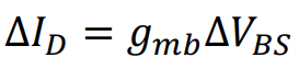
where gmb is the body transconductance or back-gate transconductance, expressed as:
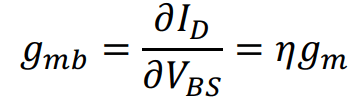
Where η is the ratio of the body transconductance gmb to the gate transconductance gm and varies typically between 0.1 and 0.25 depending on the technology.
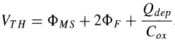
The correspondent effect of the (of the body effect) on the threshold voltage Vth can be expressed mathematically as:
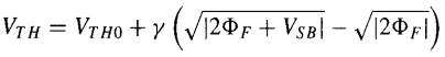
Vth0 is the threshold voltage without the effect when Vsb = 0
γ is the body-effect coefficient
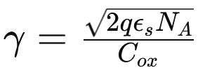
The surface potential:
![]()
![]()
More details about the formulas can be found in Razavi section 2.3
Body Effect Cancelation
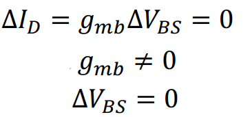
The body effect occurs because the Bulk and Source are not always maintained at the same potential. The body effect can be canceled by nulling Vbs = 0.
If Vbs = 0, the increment of drain current due to the body effect is zero, but gmb is still not zero!
The major drawback of attaching the bulk to the source is the requirement for a dedicated well for each device. This necessitates the implementation of extra guard rings in the layout and follow certain DRC rules, such as maintain a minimum distance from other devices. As a result, the layout becomes less compact, routing more complex, some extra parasitics and also the overall chip area increases.
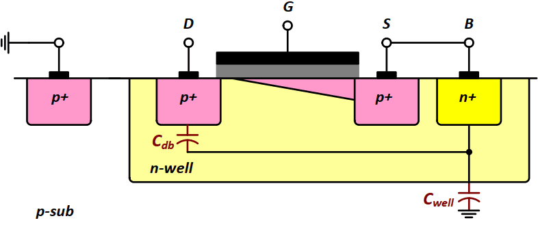
Moreover, a dedicated well for NMOS devices is not always possible. It is only possible for deep n-well technologies. However, for PMOS devices, this option is always available.
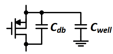
Moreover, additional parasitics due to the well (Cwell) can be calculatted arround 0.05fF/um2.
Another drawback is that the substrate noise can be injected through the Cwell parasitic capacitor. Especially digital noise can. The Cwell capacitor can coupled the noise into the analog transistors.
When Bulk => Source: A new feedthrough path from drain to Source with Cdb appears due to the drain and source junctions acting as a reverse-biased diodes. Ideally, the drain and source should never communicate, except when the gate it allows. When the device is off, a coupling capacitance Cdb is connecting drain and source, even if the gate is totally switched-off. In PMOS devices, Cdb is normally connected to vdd, and it is not problematic.
Usually, the body effect is only cancelled in well justified cases. Because, if not the previous mentioned drawbacks are more dominant than the positive effects.
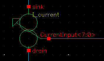
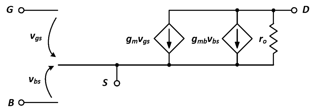
MOSFET Small-Signal Circuit Model
The hybrid-pi small signal model can be drawn including the body effect with an additional voltage controlled current source equal to gmb·Vbs. Ignoring all the capacitors (low-frequency model), the circuit is:
Example of Vth Variations
In the following circuit example, the source voltage is unequal between the devices and therefore different to the substrate. Only the first NMOS device has a zero source-to-substrate voltage.
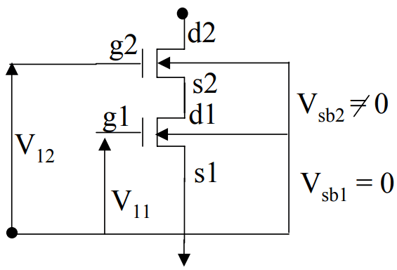
When the source-to-substrate voltage (Vsb) is increased, the threshold voltage (Vth) also increases. Therefore, in the previous example, the threshold of the second device is slightly higher than the first device.