Is it possible to integrate Inductors on-chip? What kind of inductors are available in IC? Are they feasible and useful?

Since the invention of the Integrated Circuit (IC) in 1959 from Fairchild (now ON Semi), modern technologies allows resistors, capacitors, inductors, diodes, transistors or even some kind of sensors to be integrated into a single silicon die.
In a previous article, I reviewed the kind of integrated capacitor technologies available on ICs. Now it is time for the integrated inductors 🙂
IC Inductors Challenges
Implementing passive inductors on-chip present uniques challenges as it is not as straightforward as integrating the resistors or capacitors.
- Area occupation.
- Inductors inherently are very lossy devices.
- Application at low frequencies require large inductors, which are technically unfeasible within the actual IC technologies.
- In RF applications, inductors radiate and generate strong electromagnetic disturbances that must be carefully attended.
- Inductors can not be scaled down without compromises their quality factor Q, limiting their performance in miniaturized IC designs

As you may know, an inductor is just a wire wound around a core (which can also be the air). Integrated Spiral inductors are the most common and straightforward solution. Also, bondwires inductors can be considered as “integrated” and are going to be discussed here.
Although, inductors can be implanted in the chip, they have two limiting drawbacks:
- low Quality factor
- low Henry value
In this article, the state-of-the-art in integrating inductors on-chip with spiral and bondwires inductors is going to be explained.
Planar Spiral Inductors
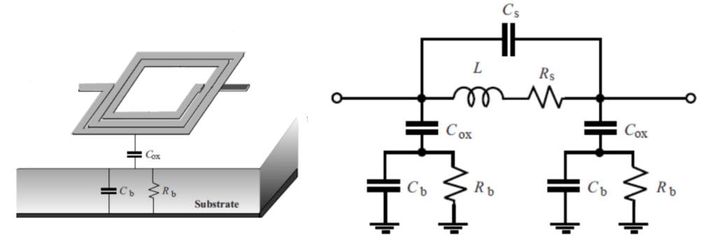
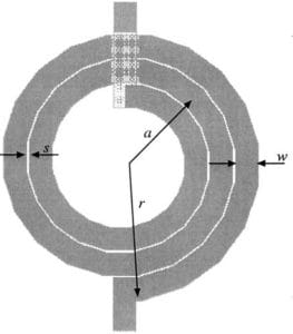
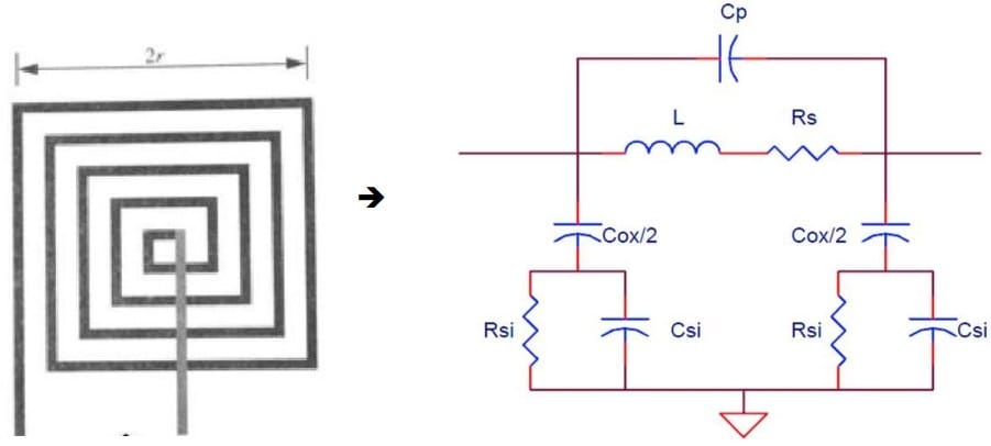
Monolithic on-chip inductors are named planar spiral inductors. These on-chip inductors are just metal lines turning around forming spires.
The value of the inductance (~nH) is increased with a larger diameter and larger number of turns.
Often they are constructed using only the uppermost layer of metal, as it offers, generally, a lower resistance to current. Although, they can be laid out forming multi-layer structures stacked vertically (more details in following section).
Single layer spiral inductors are, often, constructed using only to minimize the parasitic capacitances with the substrate, which represents the main contributor (10-30%) to the Q-factor reduction (due to the penetration of the electric filed into the substrate).
Parasitic capacitances can be reduced by keeping a large distance between the inductor layer and the substrate.
Most of the IC foundries forbidden the use of the lower layers below the spiral inductor.HH
Inductors are the most area-consuming passive component in IC circuits
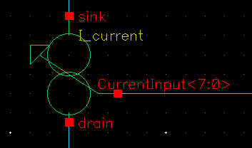
Planar inductors can achieve low inductance values, but in comparison with on-chip active inductors, they perform better in terms of linearity and a low level of noise because the only noise generation mechanism is the loss due to the series resistance and leakage.


Stacked Spiral Inductors
The inductance value can be increased significantly by using multiple layers of spiral inductors, as it can be seen in the following graph [4]. They are pilled up with various metal wires routed in spirals forming the stacked configuration.
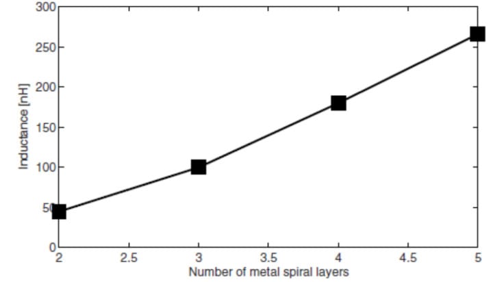
Additionally , the self-resonance frequency decrease when increase the number of stacked spiral layers.
The routing direction of the spiras in differential layer must be designed to enhance mutual inductance, thereby increasing the total inductance.

Summarizing
Low quality factor: The ohmic loss is high (specially at high frequencies) due to the resistance of the wires (skin-effect) and the resistance induced by the eddy currents in the substrate. The Quality factor is in standard CMOS is typically between 4- and 7 [4].
Low inductance: the main drawback of spiral inductors is their low inductance, however, this can be increased by adding more turns or stacking multiple metal layers. Inductance is set by the numbers of turns, and this is fixed (inductance is not tunable).
Large silicon area: Due to the previous reason, adding more number of turns to the inductances implies a greater amount of silicon area (that increase a lot the cost of the chip). They are by far the most silicon-consuming components.
Low self-resonance frequency: The area of the spira is high (due the 2 previous reasons) forming the stray capacitance also high. That means, that the self-resonance frequency is typically in the low GHz range.
Not available in all technologies: Spiral inductors are not available in low-cost digital-oriented CMOS processes.
Complex modelling: Difficult to model accurately due to complex parasitics and the lack of comprehensive libraries from the foundry.
Monolithic die with on-chip inductors
Cheap for mass production. No external components are needed.
Bond Wires
A bondwire is the connection cable used to join the pads of the silicon die to the package pins or legs of the package.
By connecting multiple bondwires between bonding pads, an inductor is created. This can be seen easily on the figure below.
This is made during the chip packaging process and since the bonding step is a must during the chip packaging, these kind of inductors do not add too much extra cost. Although, the packaging process must support internal bondings.
These kind of inductors have low loss due to gold bondwires and higher Q than spiral inductors, but much less than off-chip coils.
The cost of the bondwire inductors is higher than the planar inductors. Each bonding connection costs aprox. 0.18$ at packaging. So each turn would cost 0.32$ [3]

Summarizing
Not available in all packaging technologies: internal bounding must be support.
Dies must be packaged. On wafer testing during the development is not possible.
Higher Q than spiral inductors
The area below the pads, can be used by other part of the circuit.
Sources:
[1]: “CMOS Active Inductors and Transformers. Principle, Implementation, and Applications”, Fei Yuan. Springer. 2008. Book
[2]: “Modeling, Design, and Characterization of Multiturn Bondwire Inductors With Ferrite Epoxy Glob Cores for Power Supply System-on-Chip or System-in-Package Applications”, Jian Lu, IEEE Transactions on power electronics.
[3] “A 7.1-mW K/Ka -Band Mixer With Configurable Bondwire Resonators in 65-nm CMOS”. IEEE Transactions on Very Large Scale Integration (VLSI) Systems
[4]: A Novel Approach for Generating Active Inductors for Microwave Oscillators. PhD. Ulrich L. Rohde. Link
[5]: “An Overview of Fully On-Chip Inductors”. RADIOENGINEERING, VOL. 32, NO. 1, APRIL 2023. Link


Nice overview. Thanks for adding more recent references.
Ashis
Hi Alberto,
Do you know how to test the chip indcutor ?
Thanks!
Henry Yu
Hello Henry,
You can test it pretty similar and almost in the same way you test a regular inductor to measure de Q and L.
Best Regrds
Great stuff Alberto. You are the chosen one.
Kisses from Cambridge.
Maithri