There are many types of comparators, in this example a comparator with hysteresis is analyzed and simulated.

What is the function of hysteresis in a comparator?
By using the threshold we can reduce the glitches on the output caused by the small ripple of the input signal. When the compared voltages are similar then the output is going to flicker if we do not implement a minimum hysteresis. And, of course, multiple transitions in control signals have to be avoided.
The hysteresis is essential to compare noisy signals or similar voltages.
The schematic
The proposed circuit is based on a two-stages open-loop comparator, but adding an internal positive feedback to accomplish the hysteresis. [1] It is a differential-to-single-ended comparator with one stage output buffer (if needed, more output buffers can be added).
The basic topology can be seen in the schema:

The following 2 schematics are implemented in Cadence. Both are the same, they have just a different representation. Maybe the second representation is more clear and understandable.


In this topology, two kinds of feedback can be found with the inputs (IN- and IN+): positive and negative. The negative feedback is through the transistors M1 and M2. The positive feedback is on the transistors M14 and M15.
The ratio between M1 and M15 will determine the overall feedback sign. To have hysteresis, the ratio mult_M15/mult_M1 should be greater than 1.

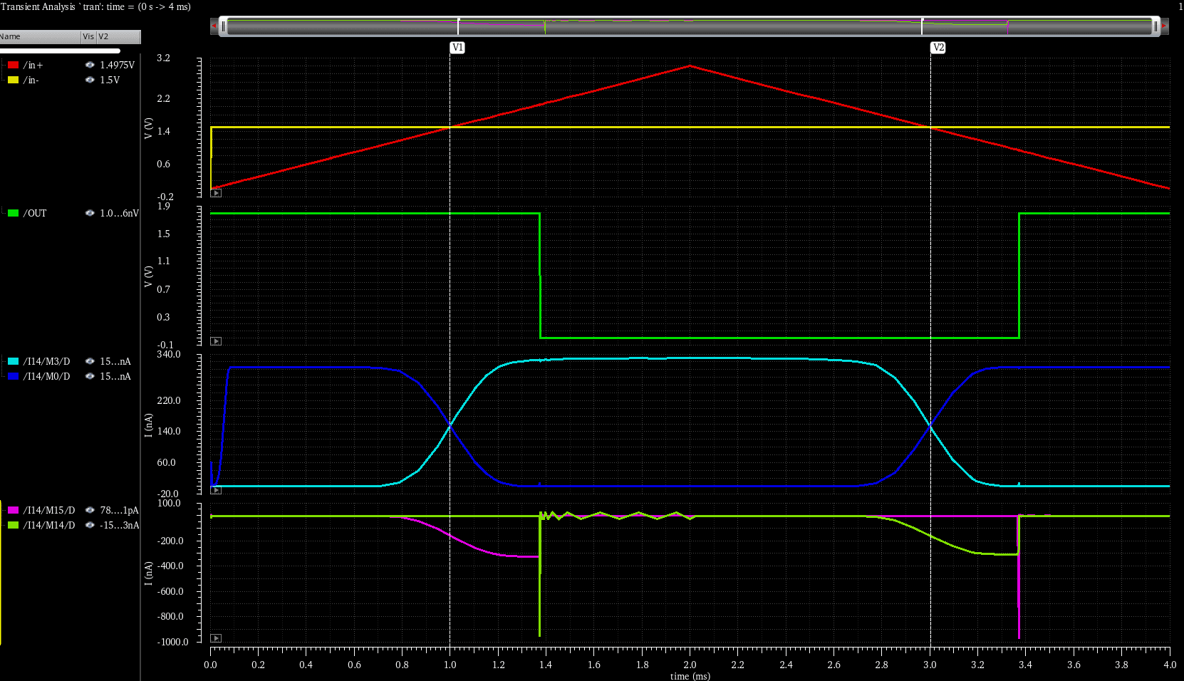
In a normal comparator, we need to consider two cases: when the currents in M0 and M3 are different but neither is zero, and when one of the input transistors has a current equal to the sink (IPOL in the following case) and the other current is zero.
Comparator Test Bench
For test the behaviour of this comparator, a capacitive load of ~1pF is attached to the output. The bigger the output cap is set, slower the response is going to be. To improve the driving capabilities of the comparator, you may only add an incremental chain of buffers at the before the output of the comparator. For my case with one small inverter was enough for the performance required.
- The bias current is set to 80nA.
- The technology used in this case is TSMC 180nm general purpose.
In this testbench, I attached several voltage sources to the positive input. By this way, I can comment out (ignore) the source I don’t want to use. So I can configure and modify the input source easily.

To see several hysteresis, I will sweep different transistor ratio between the positive and negative feedback. For that, I set a variable named “mult”, which I control how much current flow into the positive feedback.
After the simulation

We can see, that the bigger the ratio between M15 and M1 is, greater is the hysteresis.
To graphically represent the hysteresis, normally the sweeping input voltage is plotted versus the output. This shows better the called bistable characteristic.
That can be done in Cadence!! by clicking on the menu: Axis>> Yvs Y.


For the case of mult = 20, the trip voltage is approx. 1.02V and 1.98V, which can be seen better in the following graph:

Current behaviour
The current wave diagram helps a lot to understand what is happening on the comparator, here a screenshot:
One side hysteresis
For that the size of the transistor M14 was reduced to mult = 1 and the M15 was sized to mult = 20. As the following schema:
The results show how when in+ is less than I- (attached to 1.5V), we obtain more hysteresis because of the feedback of In+ is weaker


To obtain more hysteresis, you may play with the multipliers of M14 and M15, as well you may increase the length of M1 and M2 (or even M0 and M3)
[1] CMOS Analog Circuit Design. Douglas R. Holberg, Phillip E. Allen


Sentences about fb are wrong, the other should be positive: “The negative feedback is through the transistors M1 and M2. The negative feedback is on the transistors M14 and M15.”
I appreciate your correction. Yes, I wrote twice “negative fb”… fixed!
How did you decide on the transistor sizings? I would appreciate if you could also share your calculations.
Hello,
I did not save it, but they are very rough, and most of them were done based on experience. Sorry I can not help you more 🙁
Best Regards
Hi Sir,
At what points of Vout, you are calculating the two thresholds??
Hello, i dont understand the question. You can adjust and “move” the threshold depending on your design…
Dear Sir,
Please, Explain the Comparator operation.
Hello Karthick,
The circuit is comparing 2 signals with different levels to compare (hysteresis)
Best Regards
Hi Alberto,
Thanks for walking through the design. I am wondering if your comparator is clocked – because for plotting the hysteresis, I assumed for a clocked comparator, your output (OUT) should be also swinging rail-to-rail bounded by your power supply. Here, instead, I see a constant output voltage at 1.8 V when say your input is smaller than your reference voltage, and a 0 V when it is larger.
Chris
Making M14/M15 not equal size, created systematic offset. Having systematic offset makes the circuit much more sensitive for process spread.
Hi,
Thank you for a detailed explanation of the working of the circuit. I tried designing this exact same circuit on cadence but its throwing some error that goes “Analysis was skipped due to inability to compute operating point”. I am trying to solve it though.
Could you please tell me other circuits where I could apply this ? It is for my project and it needs some innovation. I wish to carry this work further and maybe integrate it in some application.
Thanks in advance.
GET PROFESSIONALLY VIDEOS AT AFFORDABLE PRICES
We offer professionally produced videos at affordable prices.
Our videos have the look and feel of a high quality television commercial, complete with professional spokesperson, background, text,
images, logos, music and of course, most importantly, your company’s contact information for your miscircuitos.com.
If you’re ready to reach more clients today, let us get to work on producing your company’s exclusive video.
MORE INFO=> http://qejn39630.bloggerbags.com/8235143/get-videos-at-affordable-prices
do u know how measure offset ?
Hi,
Thanks for your article.
I have designed and simulated this comparator, which seems to be working. However, I have one problem: the high supply voltage in my circuit. Due to this problem, some transistors will have Vds and Vgs higher than the maximum allowed voltage defined by the process. The supply voltage is 4V, and I’m using 2.5V transistors in a 65 nm process. I have tried to solve the issue by connecting a series of diode-connected devices to, let us say, break down the voltage. Still, I noticed that this solution degraded the comparator’s performance, especially since the maximum output swing is no longer possible.
Have you faced a similar problem, and how would you solve such a problem?
How do you determine the power consumption of the comparator?
hello Mohammed,
Usually you place a current probe on the gnd of the comparator and “integrate” the current during the time to calculate the average comsumption. You can calculate the consumption per cycle or the average instant comsumption.
Remember that in DC: Power = V*I
Regards
Alberto
In the test bench, what did you mean by “[commenting] out ([ignoring]) the source [you] don’t want to use”?
Also, how exactly did you implement the mult variable, and where?
Thank you in advance.
Hi,
You must press “Shift+del” in Cadence to use the ignore function. Basically, you tell the software to “ignore” and dont use that block. The positive thing is that you dont have to delete it if you want to deactivate or not use a block for some simulations.
Regards
Alberto
I didn’t know this keyboard shortcut, thanks. What about the mult variable? I don’t see any of the components with the value “mult”. Where did you put it, or what did you mean when you referred to it?
Hi, this is the multiplier of the mosfet, You can set it to 1 for an starting point.
Best Regards
Alberto
your figure is a way and your explaination mentioning the mos name based on another figure.
very confusing honestly
Sorry, I have updated the figure but forgot about the text. Will review when I have time!
Thanks
Alberto